Summary of the week
This week we each did similar programmer boards to be used in the following assignments. Although task itself was quite straighforward and clear, it wasn't very easy. First I was surprised how elegant system that "mod-webpage" is (of course also pretty complex to understand) because we did start our learning by setting up documents for milling machine by using that. When board was ready, it was time to pick-up components from storage drawer - I was surprised about the collection of the components: we can use wifi, bluetooth etc. components together with resistors, capasitors, microcontrollers tc. All these steps took more time than I had thought. Anyway, it was pretty interesting
In the second day I continued by starting the soldering. However, I had earlier experience of "old-school" soldering where components have clear legs and circuit board has holes etc. Now I had to solder by using my iPad as a "microscope" and forceps as a precision tool to place surface mountable components into correct places. Huh, this was challenging. I think that most challengig was to solder resistors, capasitors etc. single surface mounted components, because of you need one hand for tin, one for iron and one for forceps. So, actually and in practise, it's impossible equation! However, somehow I did learn correct behaviors in order to handle situation. Anyway, quality of my work does not represent perfect possible soldering, but I hope that its good enough. In my next pcb work I will try to increase quality.
TESTAUS
Overview of the programmer task
In Oulu, our task was to follow local design guidelines for programmer. Dr. Antti Mäntyniemi explained us how FabLab Oulu approach will be more convenient approach for programming microcontrollers in the future, because we can use directly Arduino toolkit and can avoid python scripts etc.
For me it was ok, I was little bit surprised that we actually did design arduino board with atmega AVR chipset. Major difference to Arduinos, which are familiar me from educational technology context, was missing contacts to external devices. Actually we were producing programmer which did use a part of Arduino functionalities for programming other microcontrollers.
In FabLab Oulu we have followed the tutorials found at in:
- https://github.com/SpenceKonde/megaTinyCore/blob/master/MakeUPDIProgrammer.md
- https://www.pcbway.com/project/shareproject/A_USB_stick_sized_UPDI_programmer.html
- https://github.com/ElTangas/jtag2updi
- https://www.electronics-lab.com/project/getting-started-with-the-new-attiny-chips-programming-the-microchips-0-series-and-1-series-attiny-with-the-arduino-ide/
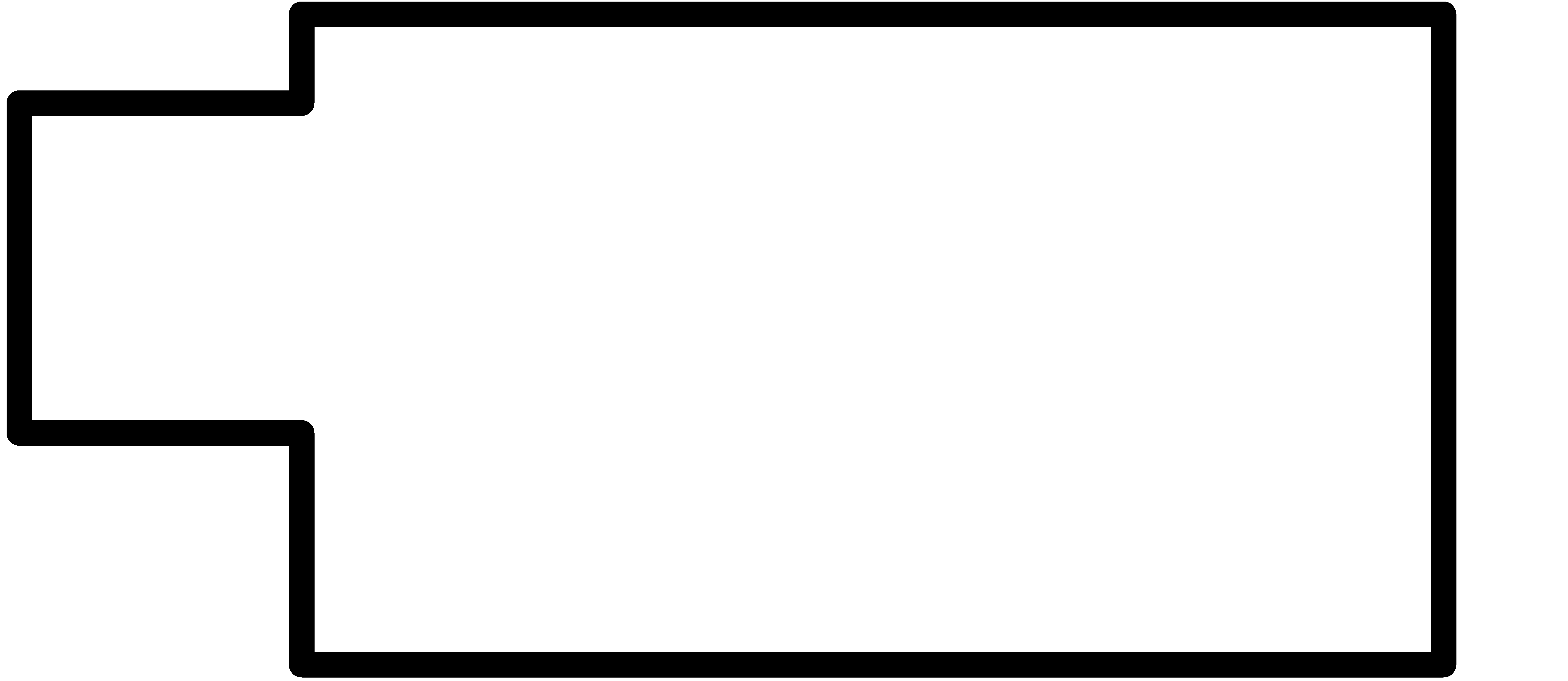
Board measures
- dpi: 2400
- px: 5932 x 2575
- mm: 62.780 x 27.252
- in: 2.472 x 1.073
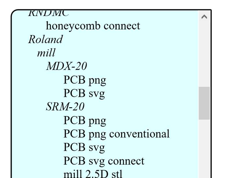
STEP 1. Creating .rml files for Roland SRM20 mill
Because we had to mill copper away from the place by using milling machine, its essential to generate accurate files for milling machine. There was two options available by our local toolkit: eagle files and png-files. Latter are meant to be used as an input to MIT Mods-system
This part explains how .rml -files were created for milling machines.
"Mods is a program generator, authored by Dr. Neil Gershenfeld of the Center for Bits and Atoms at the Massachusetts Institute of Technology. Mods produces javascript programs via a graphical user environment wherein you select nodes and graphically link them together"
Roland SRM20 needs to be programmed by creating .rml-files. For that purpose we used MODs scripts, as text below will show.
When you start with MODS' online interface (
http://mods.cba.mit.edu/) web browser seems to be empty. You will get menu by clicking right mouse button. Below is example of dialog to get PCB png module to screen:
Right-Click: Programs / open server program / Roland / mill SRM-20 / PCB png.
Three separate files were calculated by using MODs:
- Traces .rml = actual circuit board layout file
- Calibration .rml = file needed to calibrate Roland mill
- Outline .rml = file which contains outline of PCB
A. Creating .rml files for for tracing the PCB
First was calculated .rml-files for trace milling. This process of using MODs is described below
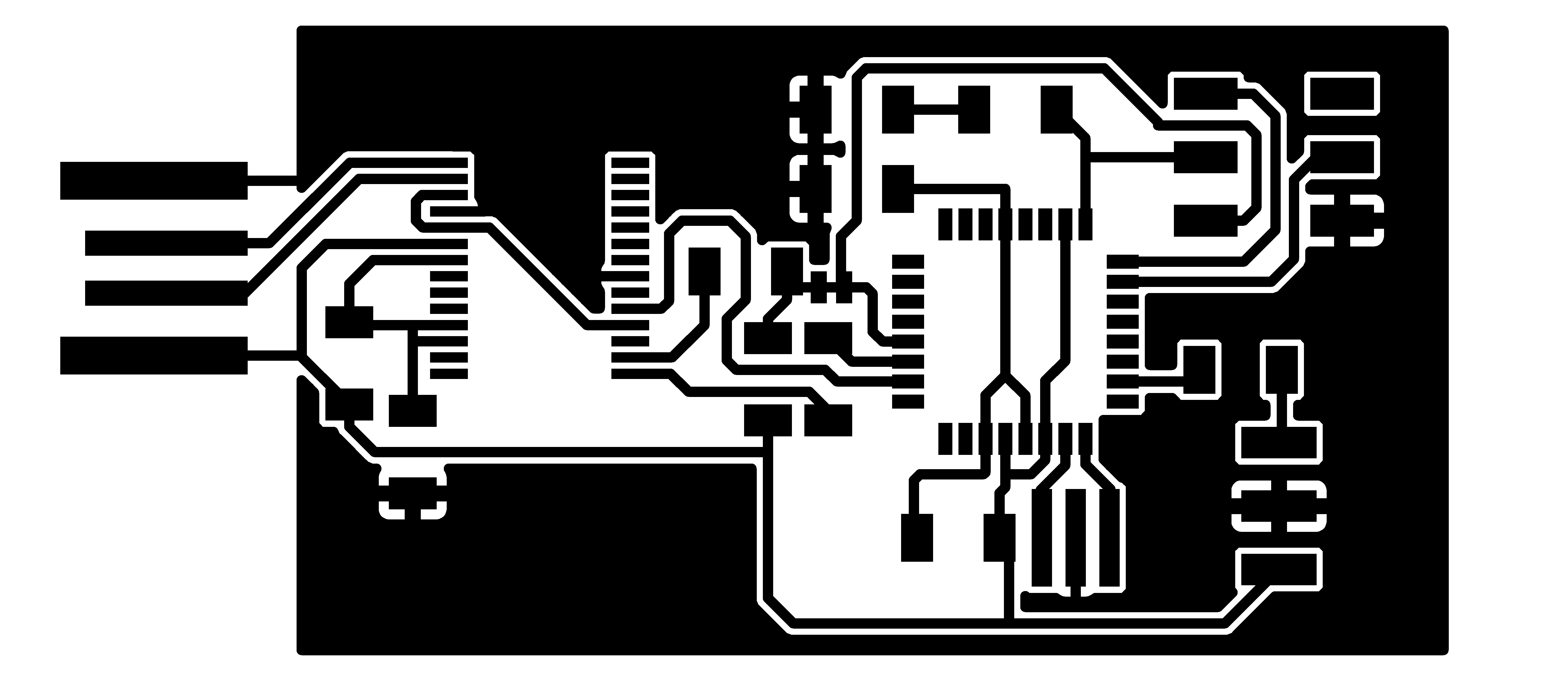
As told above, .rml files for Roland mill were calculated by using MODs scripts. In this example steps for creating "PCB tracing" are described (below the interface picture)
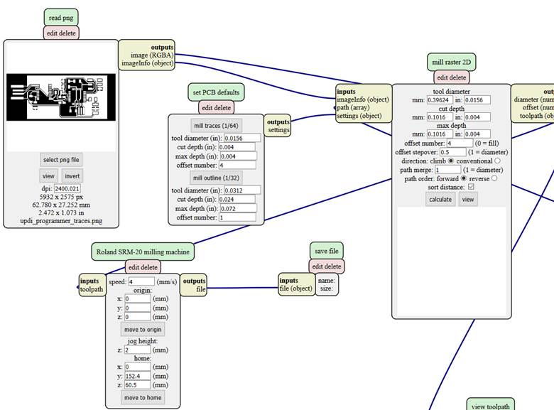
Phase 1. Settings for read .png -module:
- select .png file (download file)
- invert: machine mills the black and leaves the white.
- Check the dpi and size of the imported image.
Phase 2. Settings for Roland SRM-20 milling machine module
- Set origin (x0, y0, z0) to zero.
Phase 3. Settings for PCB defaults module
- mill traces 1/64
- 1/64 inch (0.4) diameter (especially suitable for FR1 boards) or PCB Isolation milling V tool with diameter 0.2-0.5 mm especially suitable for FR4 boards.
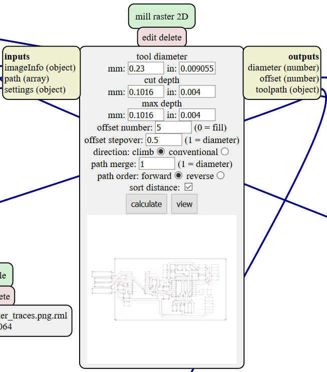
Phase 4. Settings for mill raster 2D module
- set tool diameter to 0.23mm.
- Set cut depth to. 0.1mm.
- set offset number to 5.
- set offset stepover to 0.5.
- Press the calculate button
- Finally, save the .rml file! (if you don't have time to generate .rml-file, you can try with this)
B. Creating .rml files for for calibration of the Roland SRM20
Second step for creating .rml-files was to calculate milling for calibration marks. Calibration process is explained in the phase were actual drilling is explained. Here focus is put on .rml-files
.png)
Phase 1. Settings for "read .png" -module
- select png file
- invert: machine mills the black and leaves the white.
- Check the dpi and size of the imported image.
Phase 2. settings for PCB defaults module:
Phase 3. mill raster 2D module
- set tool diameter to 0.23mm.
- set cut depth to. 0.1mm.
- set offset number to 5.
- set offset stepover to 0.5.
- Press the calculate button
- Finally, save the .rml file!(if you don't have time to generate .rml-file, you can try with this)
C. Creating .rml files for PCB outline
Last .rml- file was calculated for cutting PCB board from larger body of material
Phase 1. Settings for read png module
- select png file
- invert: machine mills the black and leaves the white.
- Check the dpi and size of the imported image.
Phase 2. Settings for PCB defaults module
- milling bit for cutout: 1/32 inch (0.79 mm) diameter or similar bith with up to 1.00 mm diameter.
Phase 3. Settings for mill raster 2D module
- set tool diameter to 1mm.
- Set cut depth to 0.6mm (The cut depth was set to 0.6mm, which means the milling bit accomplishes the cutting process within three rounds, cutting 0.6mm deep in each round)
- set offset number to 1.
- set offset stepover to 0.5.
- Press the calculate button
Finally, you can save your .rml file (if you don't have time to generate .rml-file, you can try with this
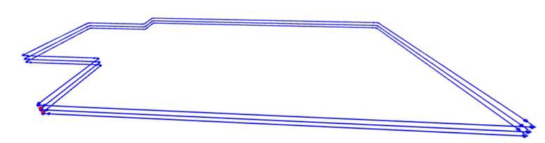
Hox! If you click "view" the calculated output can be explored from different perspectives by dragging the mouse while holding the right click button. See the figure below
STEP 2. Use Roland SRM-20 milling machine to drill and cut PCB board
For milling we used a Roland SRM-20 milling machine. Roland company claims that SRM-20 is the easiest and most precise CNC mill in its class. It is easy to believe, because machine looks comfortable and easy. However, I found that using that machine has a lot steps and for beginner it feels little bit fragile and complicated tool to be used. Definetely I have to use it many times to learn to use it adequately. Now I feel that my skills are not good enought with Roland SRM20.
Phase A. Prepare PCB board for milling
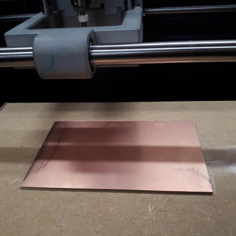
Material for programmers' PCB was FR1, which is a hard, flat material which consist of a thin layer of copper oven non-conductive phenolic resin.
First PCB board material (FR1) was cutted into smaller piece, and then it was put onto "sacrificial board", and position was fixed with doyuble-sided tape. Because Copper layer of circuit board is about 0.03mm, so it is important to keep the board flat when we manufacture PCB. That's why double-sided tape was carefully applied without overlapping each other and PCB board was inspected for any elevations or other residuals from cutting wasn't left.
below you see how pcb board is attached firmly into bottom plate
Phase B.Insert milling bit into Roland SRM-20 machine
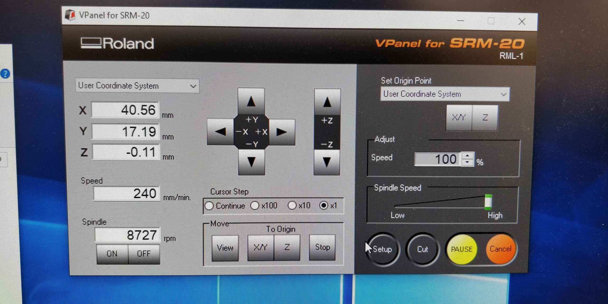
First, program ‘VPanel for SRM-20' was opened to set the origin of Z-, X- and Y-axes:
- Then the head was moved to the View position so that it moved to the center and it was easier to install a milling bit.
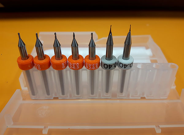
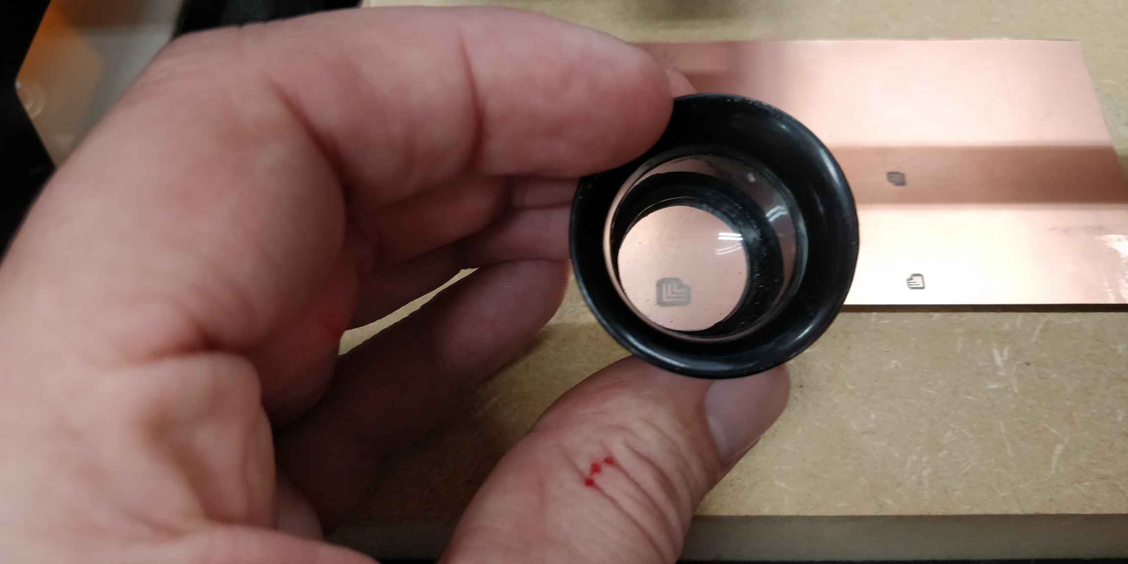
- the small screw was loosened in the shank by allen key, and then the orange v-shaped milling bit was put (size 0,2-0,5 mm) in all the way up to colored neck, and the small screw slightly fastened to fix it. [The grey milling bits in the picture were flat bits.]

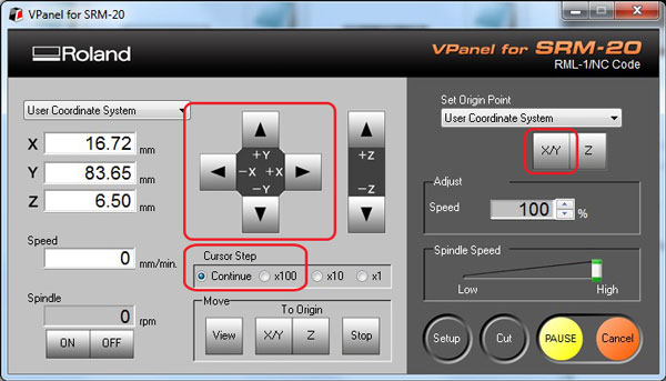
Phase C. Define the origin of Z-, X- and Y-axes
- X- axis moves the table, and and Y- and Z-axes move the head.
- Move the axes manually by the VPanel arrows with appropriate Cursor Step.
- Continue moves as long as you push it, by which you will move near to the aimed origin.
- x100 does smaller steps to get closer and
- x10 0,1 mm steps to get nearby the surface.
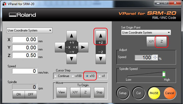
First of all, move the Z-head carefully near to the surface. In the picture below, z-head is calibrated again after failure of loosing x-asis accidentally (described later, now image is presented as an example of moving Z-head close to surface of PCB
Adjust X- and Y-axes (with the Cursor Step: Continue, and x100) and reset them to be a new origin by Set Origin Point and pressing X/Y.
Hold the milling bit with one hand, loose the screw with another, and move the bit right on the surface of the board, and then keep the milling bit still so it can't move up when fastening the screw again. Remember to not tighten too much in order to avoid ruin the milling bit body surface.
Now, reset the Z-axis to be zero by Set Origin Point and pressing Z. In order to let the milling bit turn on and speed up freely, move the Z-axis just a little bit up (around 5 steps with the x10) so, don’t leave the milling bit to the surface. Now, the machine preparation is done.
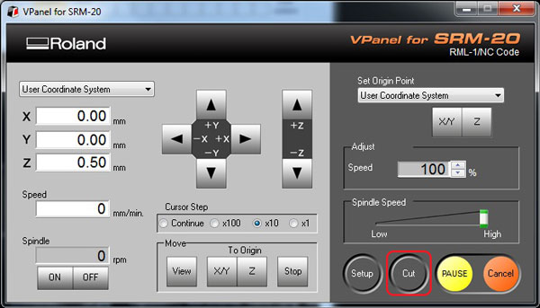
Phase D. Control milling with VPanel software
First, open VPanel software for adding .rml document and starting cutting
Calibrate mill by starting with calibration .rml
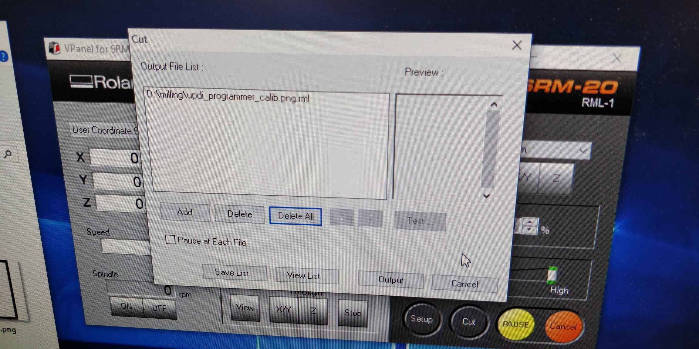
- Because Roland drilling machine is already prepared for the task (if you completed earlier phases), just go to Vpanel and select Cut.
- From the opening window, select Delete All from the Output file list and then, Add new one by navigating the "calibration.rml" and open it.
- When you press Output , everything else has to be done, since it will start cutting straight away.
Check the quality of the milling and calibrate machine my adjusting z-value (see below)
Z-axis (milling bit) needs to be adjustet until cutting quality is good enought. Picture below shows that values were changed by using smallest steps and final value was 0.11mm. If you don't calibrate Roland milling machine, please be prepared to manufacture PCB board multiple times.
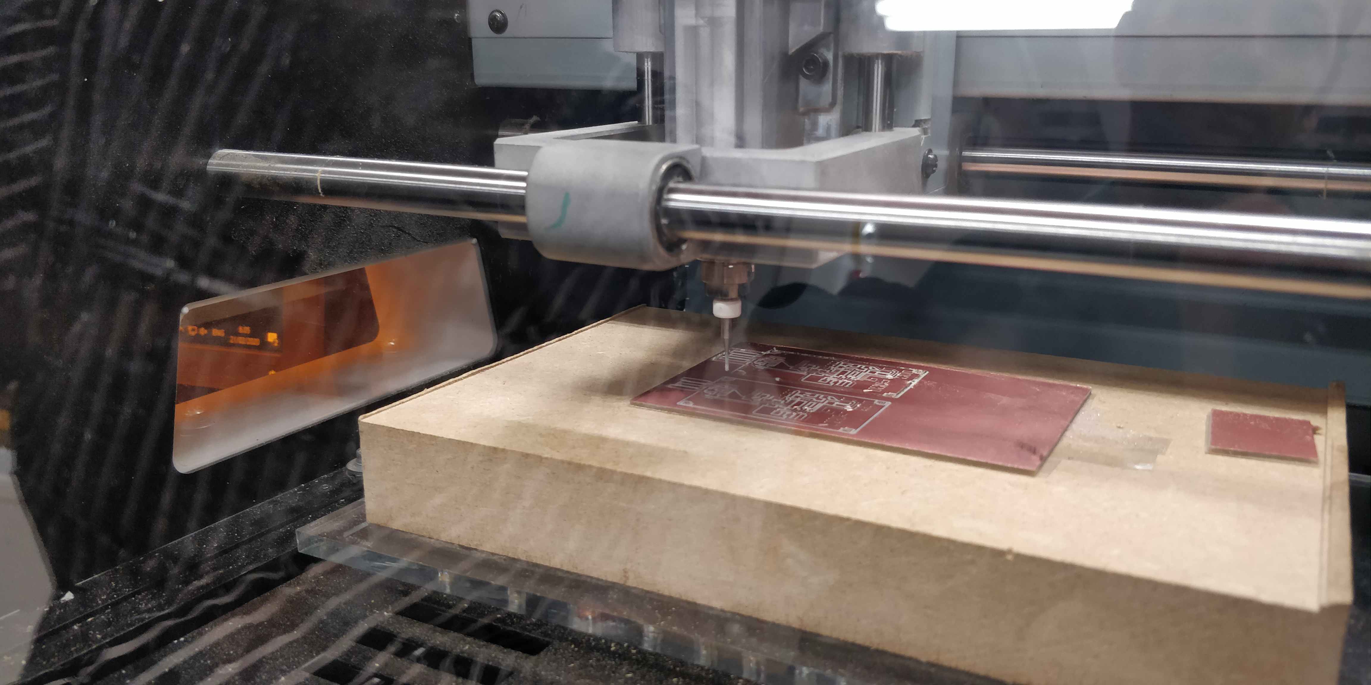
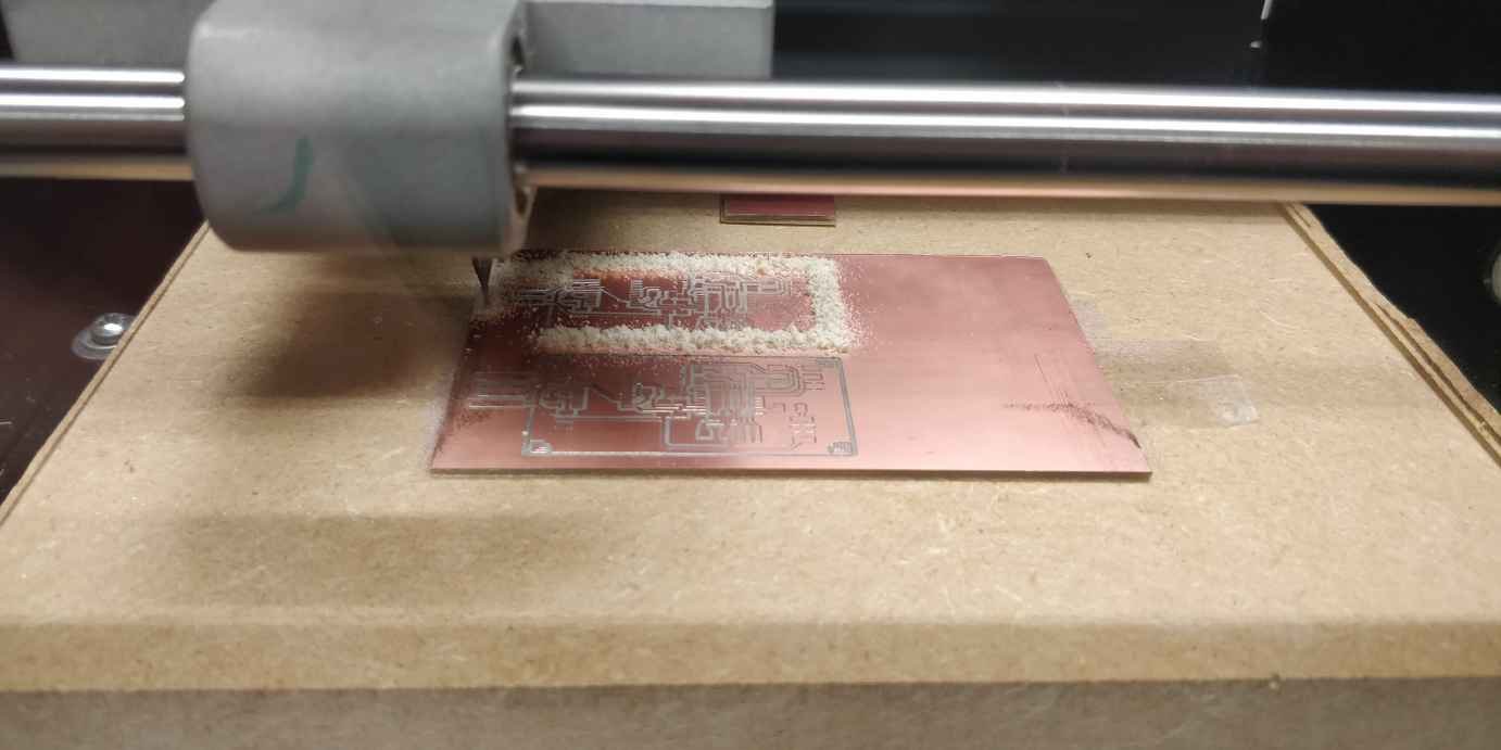
Mill traces to PCB by starting with traces.rml
- Because Roland drilling machine is already prepared for the task (if you completed earlier phases), just go to Vpanel and select Cut.
- From the opening window, select Delete All from the Output file list and then, Add new one by navigating the "traces.rml" and open it.
- When you press Output , everything else has to be done, since it will start cutting straight away.
Cut board off the PCB plate by using outline.rml
After the machine was calibrated to traces milling and traces are cut , without touching the origin, open the door of the machine, clean it by a vacuum cleaner and, remove the first milling bit.
Milling bit will be changed, so that's why you need to remove it. Change the milling bit to 1 mm bit.
Repeat the steps done for the first .rml file for cutting the outline and being able to remove the cut board from the sheet:
Do not make any changes for X/Y-origin, but find the Z-axis Origin Point:
- Move the Z-head and the milling bit near the surface of the board,
- Loosen the screw in the shank by allen key for letting the bit fall and touch the surface,
- Fasten the screw by holding the bit still so it won't move up when fastening, and
- reset Z-axis.
- Then again, raise Z-axis and the milling bit slightly from the surface and start cutting
In VPanel, select Cut. From the opening window, select Delete All, then Add new one by navigating outline .rml file and open it.
LESSONS LEARNT: How to survive of losing y-axis when you are milling multiple PCBs
I made this PCB together with my Fab Lab coursemate Yazan Barhoush. So we actually shared the task and controlled Roland milling machine together. While one PCB board was exciting enough to be milled, was the moving Y-axis (30mm) after first pcb board was outlined, more than exciting. As a result, we almost destroyed one of two PCBs (milling of outline was under the threat)
What we actually did? Well, after first PCB was outlined and we had to move Y-axis 30mm, we ended up to press "view" button in Vpanel controller.
But what does it matter?
It did reset values, in practise we had to tell x/y/z values again and how to fix those values to first PCB already outlined?
Dr. Antti Mäntyniemi showed his expertise by solving this failure. He used calibration marks (see above phase: calibration) to calculate central point between PCBs and from that it was pretty easy to estimate starting point for outline milling of second PCB while we already knew that distance between starting points was 30mm.
And everything worked!!
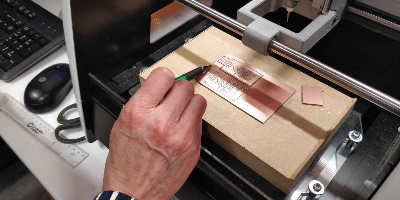
Image below shows that everything went well altough we almost destroyed our work so far :)
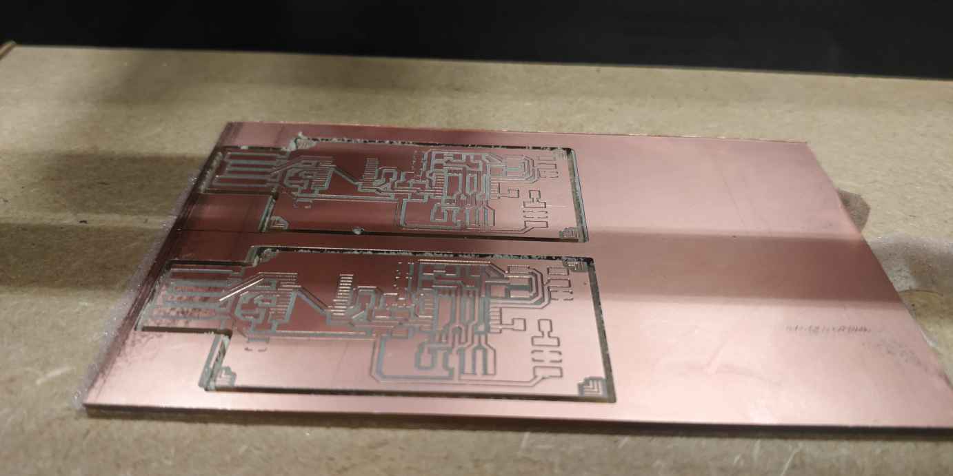
After cutting, clean and remove the cut board carefully, and clean the milled board from dust by rinsing it under the water.
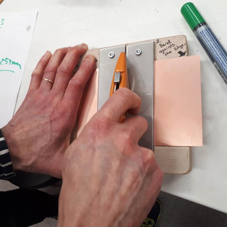
After this phase, use sharp knife to remove additional copper next o USB connector.
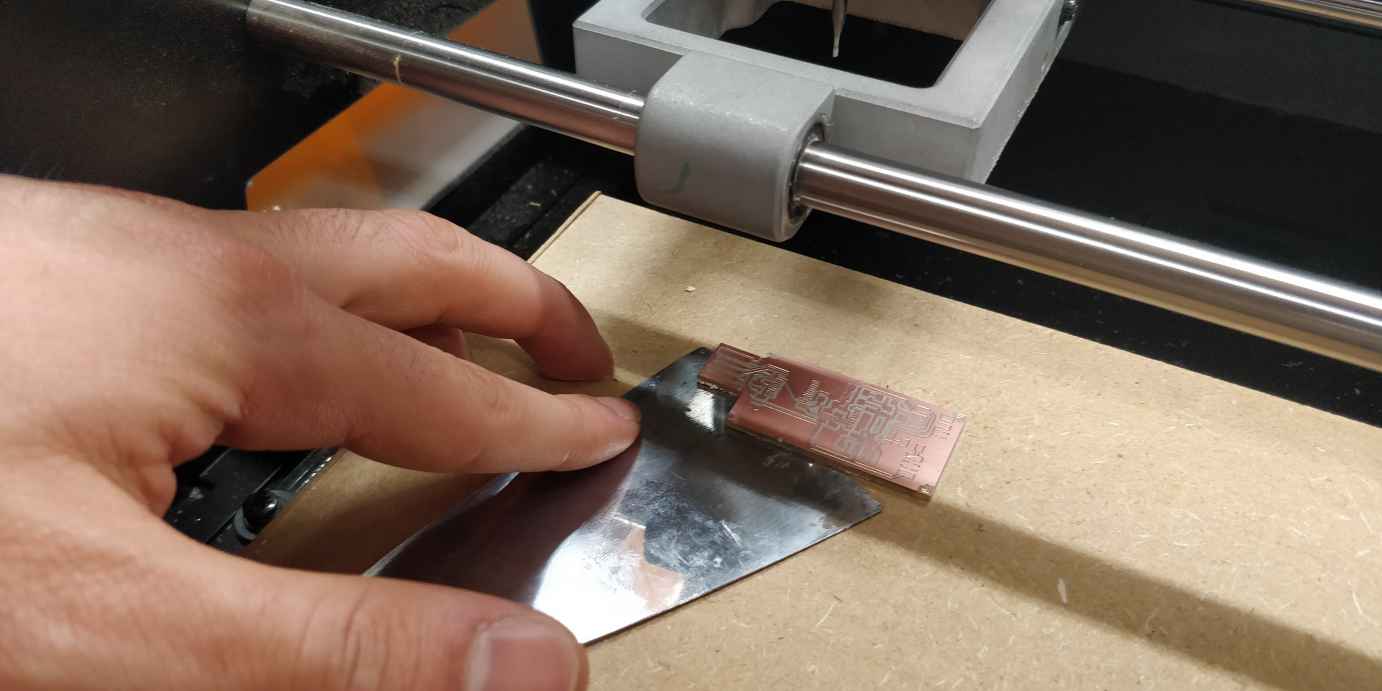
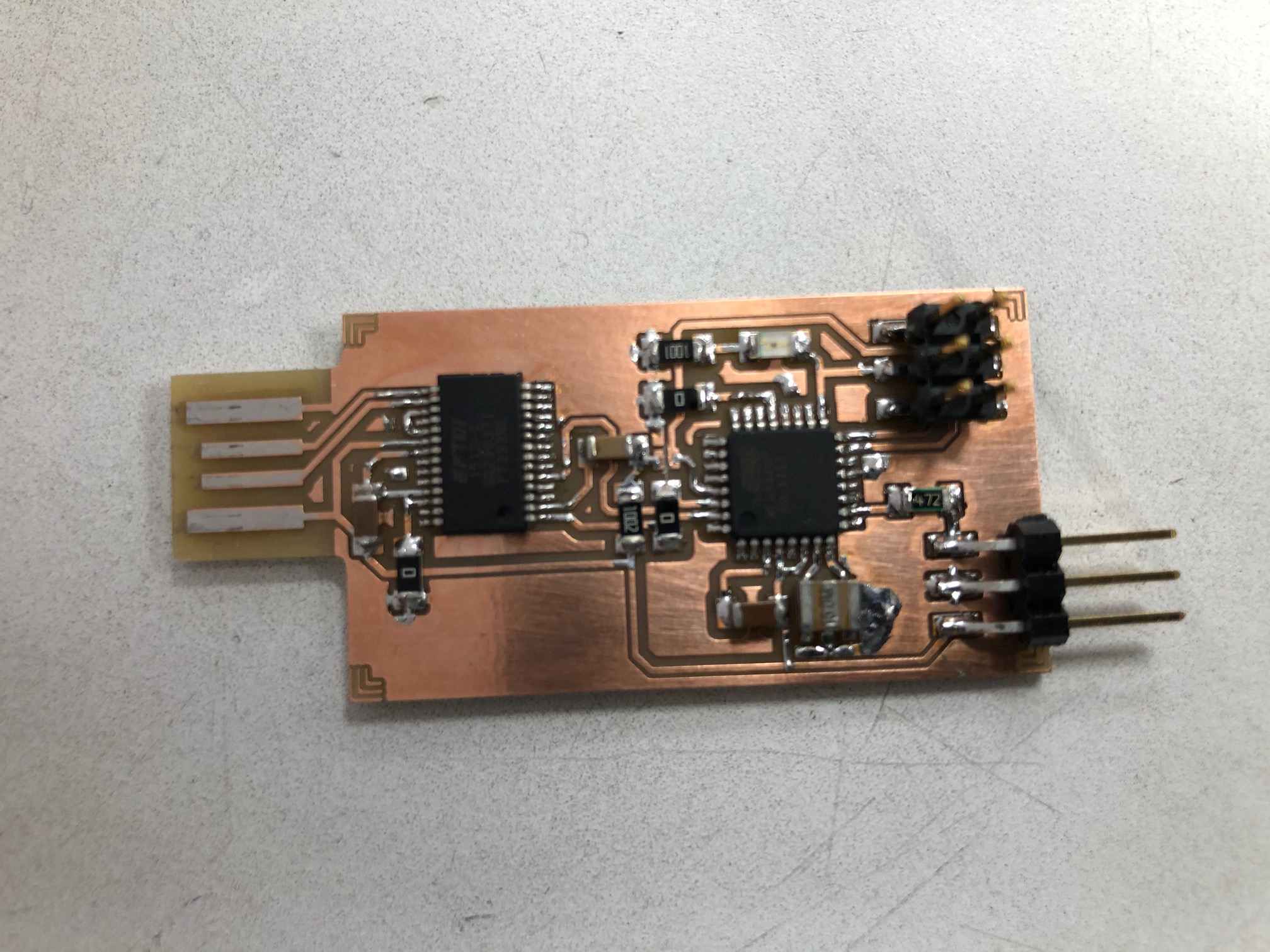
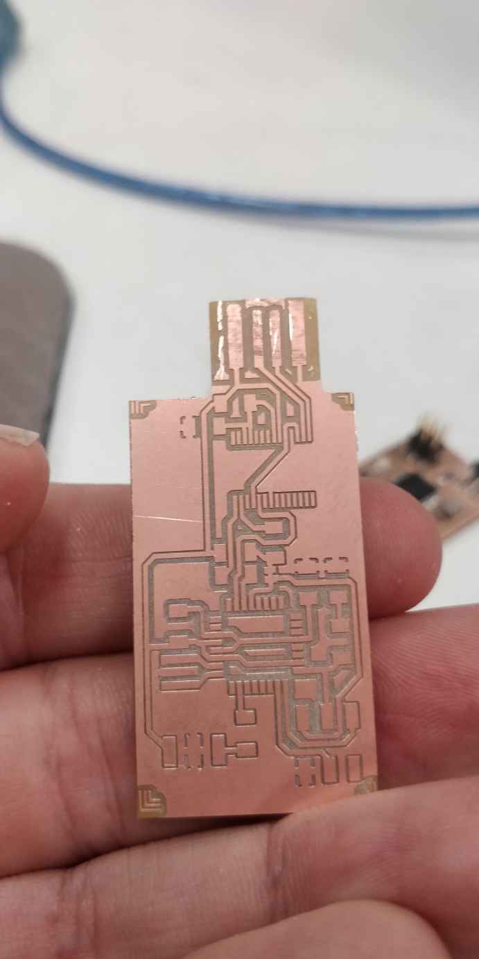
Circuit board is now ready for soldering! Great!
STEP 3. Get the components and assemble PCB
After the PCB was milled, next step was to get components to be soldered onto circuit board. I had soldering experience, but I had forgotten almost anything, so this was pretty exciting exercise for me.
Phase 1. Get list of components needed for assembly
Next task is to get list of the required components. One way to see components is to use Eagle design -software to look at schematics and list of the components.
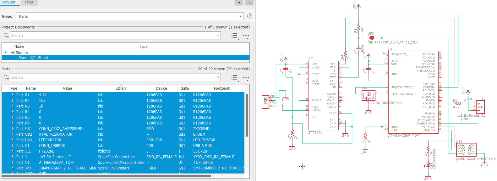
Another, not recommedable way, is to use random diagram that is just left next to component drawer. I used that, before I heard about Eagle -approach. I think that Eagle's list of the components might have been much much easier to follow
Well, I did compare that blurry diagram and drawers of the part storage. It took a lot of time, but maybe it was good to learn what kind of components are available and how to interpret "not-so-good-diagrams"
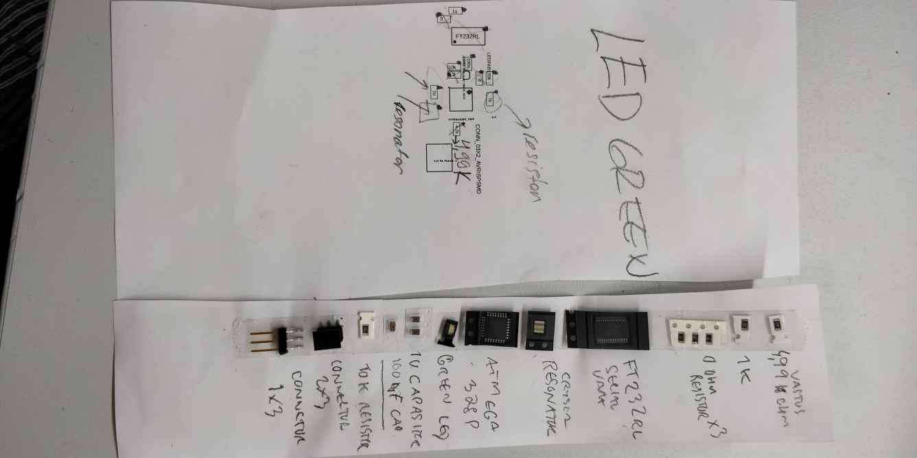
As a result of searching components, you should have following set of the parts before starting soldering:
ATmega328P - 1x FTDI FT231XQ-R - 1x green led - 2x 1uF capacitor - 1x 0.1uF capacitor - 1x 4.99 kOhm recistor - 1x 1 kOhm recistor - 1x 10 kOhm recistor - 3x 0 Ohm recistor - 1x 2x3 pin header - 1x 3RA
Phase 2. Preparations to be done before soldering
First of all, collect the tools needed: soldering iron, soldering tin, desolder braid, tweezers, and microscope, and wet the sponge of soldering iron for cleaning the tip of the iron.
Preparing to start soldering, turn on:
- the main switch and the power of soldering iron, and waited for the temperature of it to be 350 °C.
- the two main swiches for flexible “stayput” arm removing the fumes and gases caused by soldering.
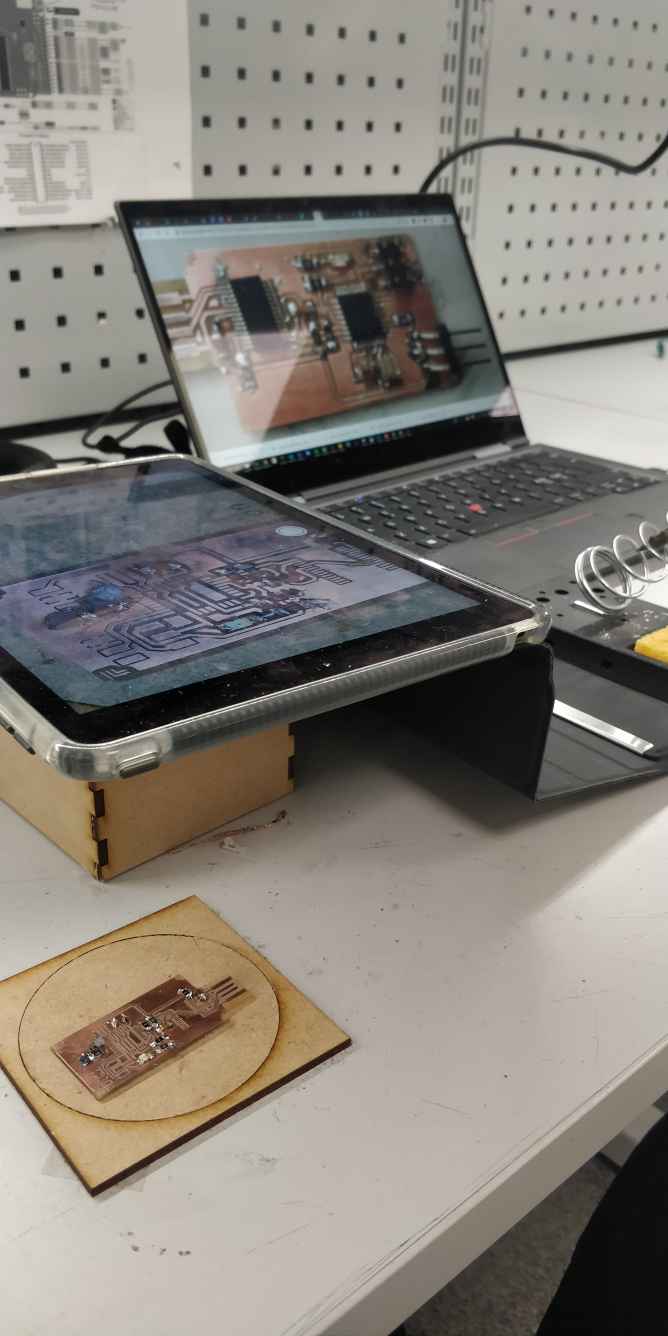
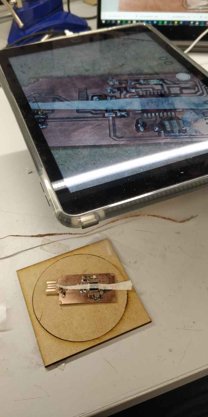
Because FabLab Oulu has only one microscope to be used when surface mounted components are soldered, following configuration is recommended: 1) lasercut box with turntable (see picture below) and 2) use box as a mobilephone or iPad holder. I recommend iPad, because it has bigger screen, so you can use it as a substitute for microscope (don't except too much still).
If you have laptop available, I recommend that you use it as a tool to show example of soldered board. It did help me, because I was able to check place of components etc just by looking briefly my laptop
Phase 3. Start actual assembly of the components
Then, you need to figure out the order of soldering the components to the board. Personally I had somekind of soldering experience, but this was my first time with surface mountable components and thatswhy pretty exciting.
However, I was instructed to start with smallest and easiest, like resistors which have also two connection joints. However,in the earlier years some students have got also instructions like that:
the hardest to the easiest
the lowest to the highest
the middle to the edges
Because I was so unexperienced of using "microscope" with soldering, I did choose approach "start with the smallest and easiest" and I think it was good approach to get little bit experience of surface mountable components before starting to solder ATMEGA controller and other components with multiple joints.
When I had soldered almost all smaller components, I had enough encourage that I was able to start soldering legs of ATmega328P
In the picture you can see, how I recommend to attach this chipset before soldering. It is very crucial to align controller to footpads very carefully. Otherwise it is risk of resoldering everything! You have been warned
That USB-SERIAL chipset FTDI FT231XQ-R seemed to be much more complicating artefact to be soldered well. I can admit that I was little bit hurry and thats'why I used too much tin while soldering legs. When legs went into shortcircuit I tried to solve issue without using tin removal copper. Instead, I tried to use soldering gun as "a knife" or "a pen" and just remove tin by heating
I don't recommend to rush with that kind of components. In my case some part of copper film overheated and popped out of the PCB. Antti Mäntyniemi was able to use his "soldering gun macigk" and we got happy end overall
Phase 4. Start to Debug! Debug! Debug! Debug! Shortcircuits are not allowed
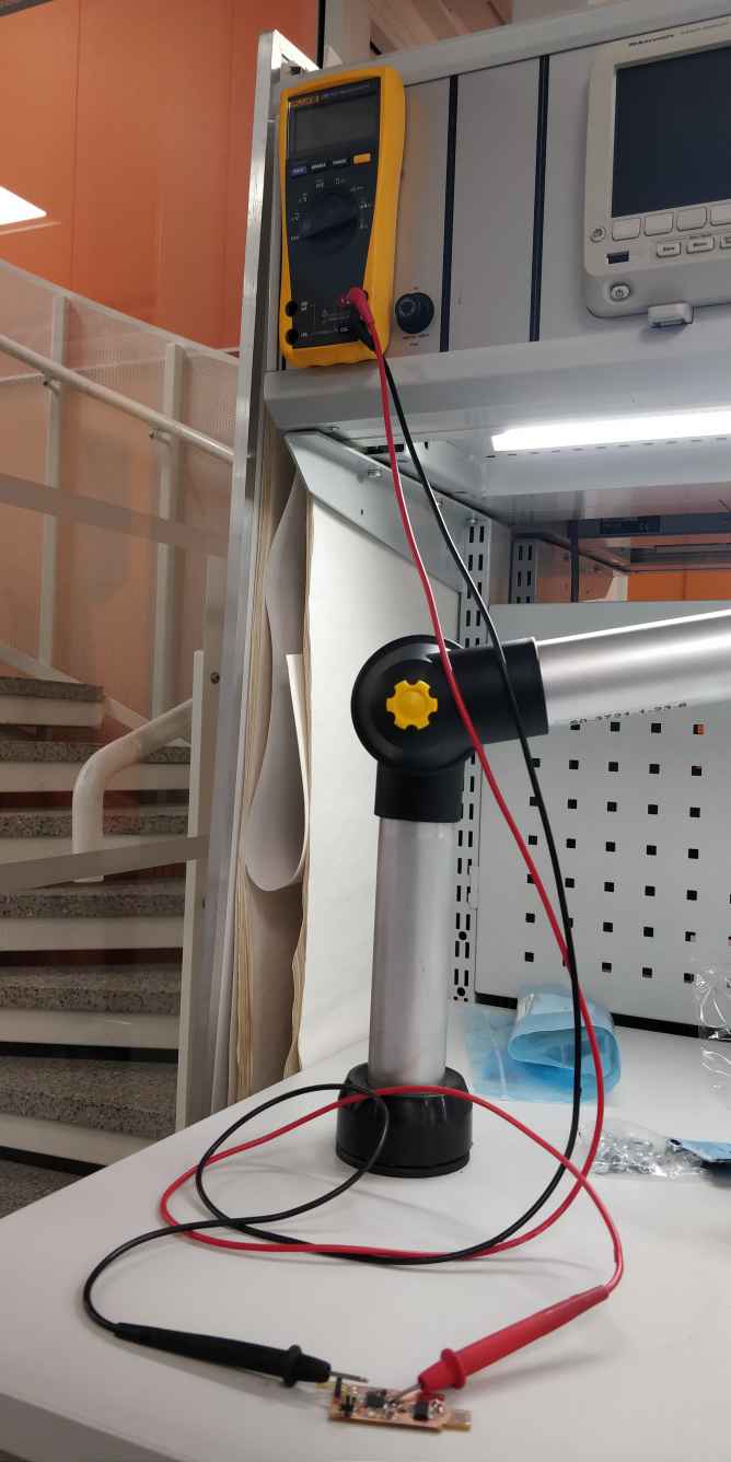
When assembling is finished, test circuitboard by using multimeter. This is very important step, because if connections are shortcut (between Vcc and GND) you can even break USB port of your computer. Of course its "worst case scenario", most often your board just doesn't work.
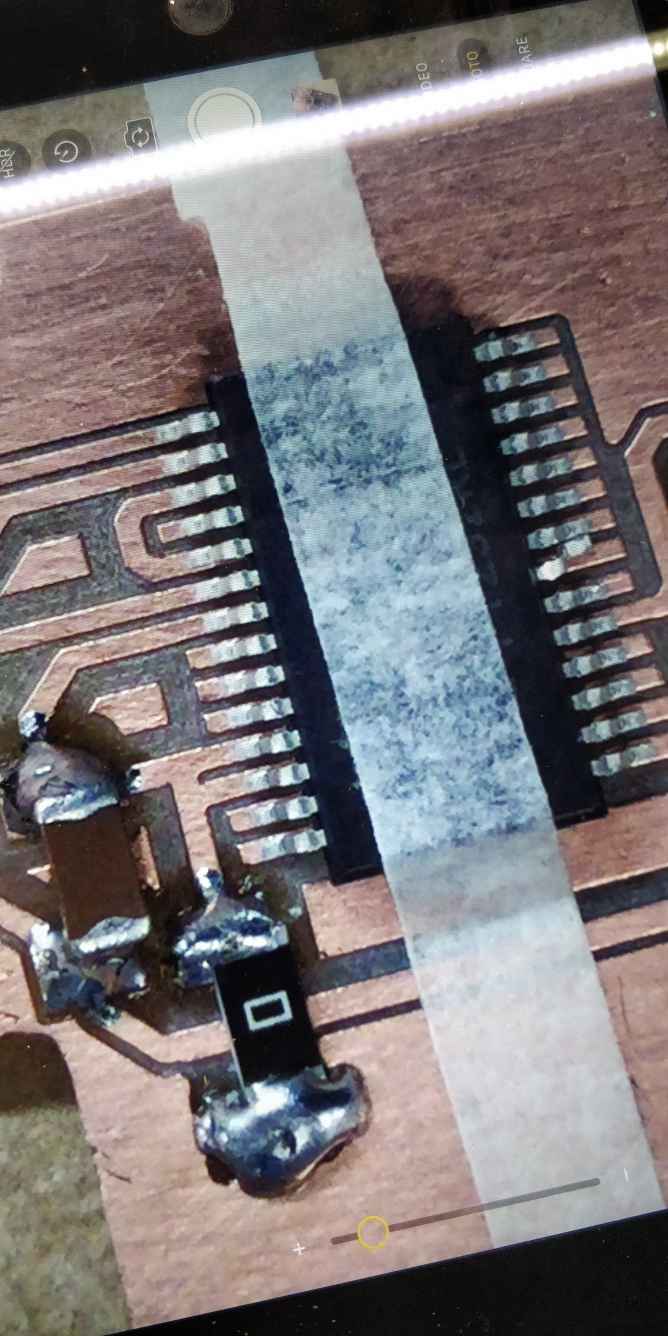
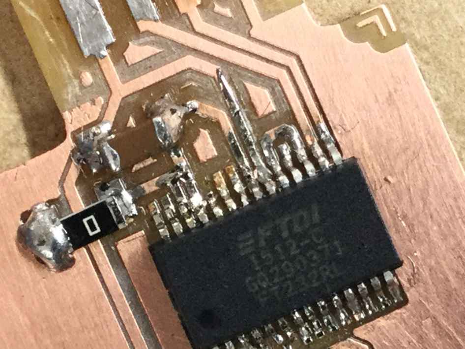
I was pretty sure that my board has shortcuts there and here, because I had been in hurry when soldering USB-SERIAL conversion chipset (FTDI chip). I wasn't surprised when connection between USB-connector and FTDI was shortcut. See the image below to get impression what was situation while I was soldering legs of FTDI
By using copper stripe for tin removal and re-soldering legs situation got better, better, better and better. FInally connection between USB-connector and FTDI was established, but bootloader upload process wasn't successfull
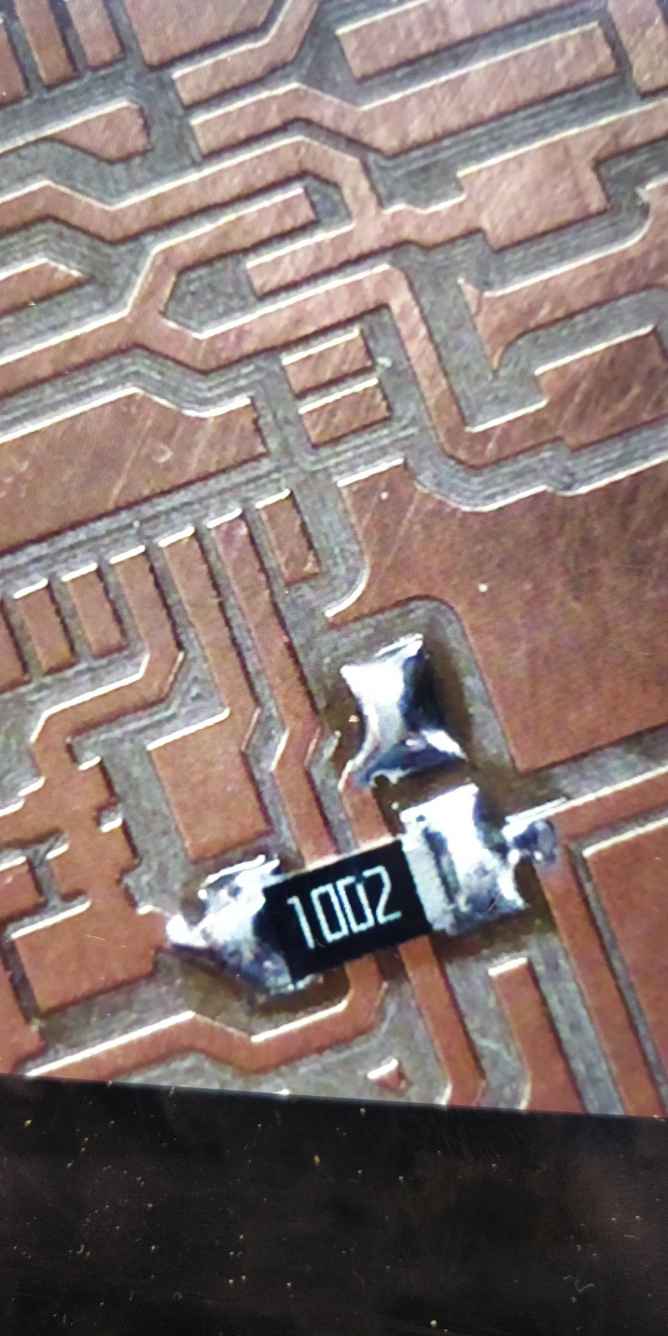
Last issue was with resonator where one leg (ground) was forgotten to solder at all. While I did solder it, i accidentally put very thin residual of tin to one side of resonator, which did shortcut it (suprise shortcut). It was very difficult to debug, coz tin residual was difficult to recognize even by using microscope to zoom the view
Finally board started to work as excepted! So happy I am!
STEP 4. Program the programmer
Programming the programmer was started by connecting PCB board to USB port (to get power) and to ATtiny microcontroller (FabLab property, used for programming the programmer). This phase was done by the facilitator, because the world of Arduino, Attiny etc. was mystery for most of us.
Workflow in the Arduino IDE (tools menu openeded) was as it follows:
- Choose Board: Arduino Nano
- Choose Processor: ATmega328P (Old bootloader)
- Choose Serial port (COM port): COM __ (replace __ with serial port used in your case [check it from device manager if you are using windows]
- Choose Programmer: USBTinyISP
Then choose from "tools" menu: burn bootloader (jtag2updi programmer)
Then board was tested by using default examples from Arduino IDE (File > Examples > Basics > Blink). Because this sketch was working after it was uploaded to board, board was working as Arduino -board
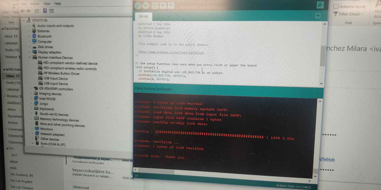
Installing the megaTinyCore
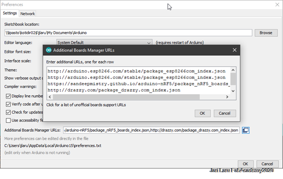
Next I used this instruction to install the megaTinyCore on the Arduino IDE via the Arduino Board Manager.
First I opened "preferences" dialog (file > preferences) and added "http://drazzy.com/package_drazzy.com_index.json" JSON file to get board information. It was added via "additional board manager urls" -dialog.
Next I openeded Arduino Board manager (Tools > Boards > Boards manager) and entered megaTinyCore into search bar. When I got right package, i clicked install.
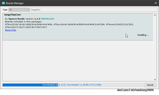
Then I did search for "Arduino megaAVR board" and installed the most recent version of that too.
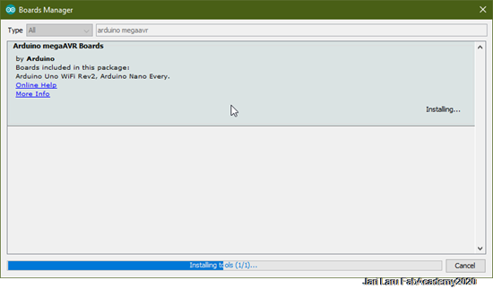
I checked that the board installation was succesful by checking are Attiny boards listed in the boards list (tools > boards)
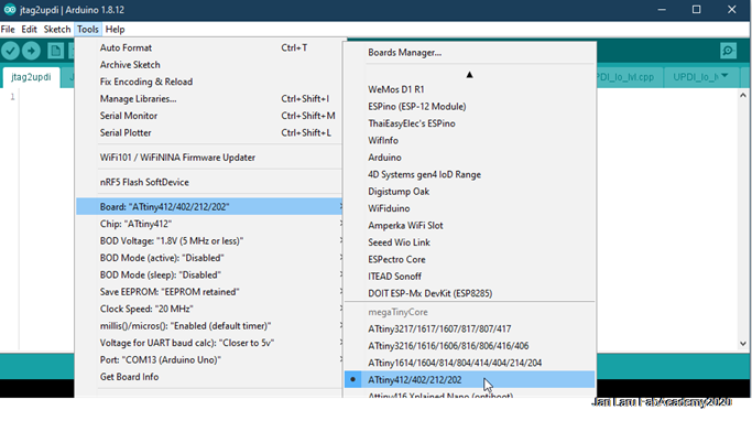
Configure it to work as a UPDI programmer
I downloaded UDPI programmer sketch (SpenceKonde / GitHub) (zip file) and extracted it.
I did extract zip-file and opened jtag2updi.ino sketch (screen looks to be empty, but all required files are linked to it) and then uploaded it to my programmer board
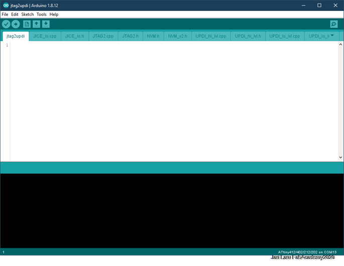
I did upload jtag2updi.ino sketch by using following settings:
- Board: Arduino Nano
- Processor: ATmega328P (Old Bootleader)
- Serial port: You have to check it from device manager (if you are using windows)
- Programmer: AVRISP mkll
When Arduino IDE showed "DONE uploading", my board was ready to work as a UDPI programmer.
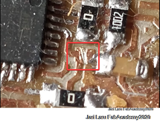
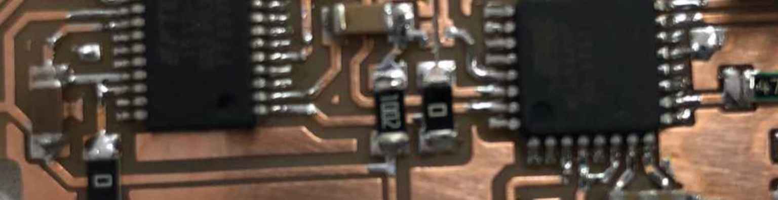
Now it was time to cut connection between USB-SERIAL (FTDI) chip and microprocessor. In the picture below you will see the part of the PCB where connection is scratched off by using knife.
Test the programmer
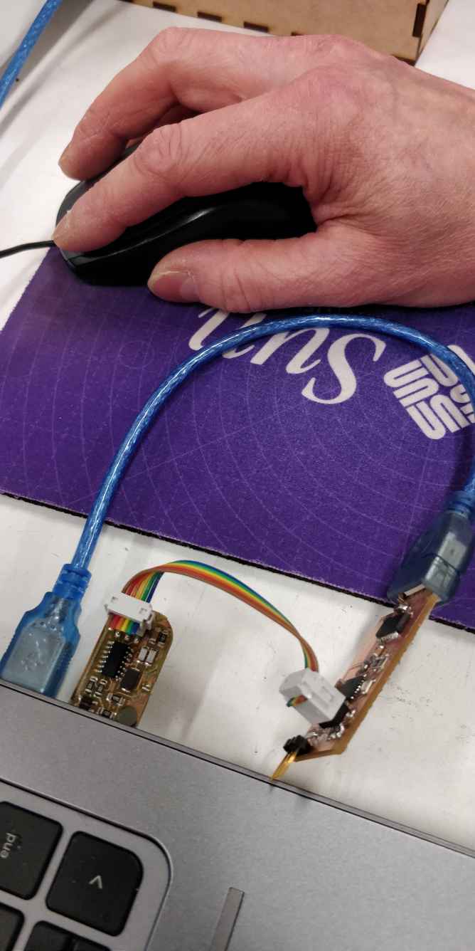
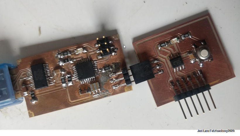
Because I finalized this documentation later on, I was able to use PCB done in the "electronics design" week for testing the programmer.
I connected that board to UPDI connector of the programmer, but before that I checked that both board are working as planned (no shortcuts and that scheme/board design are correct)
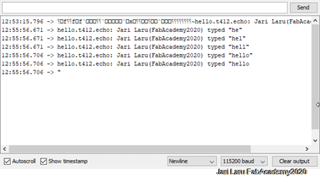
Next I opened echo.ino code by Neil Gershenfeld in Arduino IDE, added my name to it and clicked UPLOAD
//
// hello.t412.echo.ino
//
// tiny412 echo hello-world
//    115200 baud
//
// Neil Gershenfeld 12/8/19
//
// This work may be reproduced, modified, distributed,
// performed, and displayed for any purpose, but must
// acknowledge this project. Copyright is retained and
// must be preserved. The work is provided as is; no
// warranty is provided, and users accept all liability.
//

#define max_buffer 25

static int index = 0;
static char chr;
static char buffer[max_buffer] = {0};

void setup() {
   Serial.begin(115200);
   }

void loop() {
   if (Serial.available() > 0) {
      chr = Serial.read();
      Serial.print("hello.t412.echo: Jari Laru (FabAcademy2020) typed \"");
      buffer[index++] = chr;
      if (index == (max_buffer-1))
         index = 0;
      Serial.print(buffer);
      Serial.println("\"");
      }
   }
Then I opened serial monitor in Arduino IDE (with the same baudrate (115200) than specified in the code above). Code works succesfully, as you can see from the image below:
What I did learn from this exercise?
This week was very exciting experience, because PCB board were milled by using Roland SRM-20 machine. It seemed pretty difficult to get proper PCB from that milling machine. Well, after all, I did succeed to use that machine.
I had previous experiences of programming and soldering, so I wasnt' afraid of those parts of the week. Anyway, electronics seems to be pretty exciting field!
Files:
- PNG Files
- RML-files for milling